Exploring Possibilities: A Holistic Approach to Materials Processing for Scaled Devices
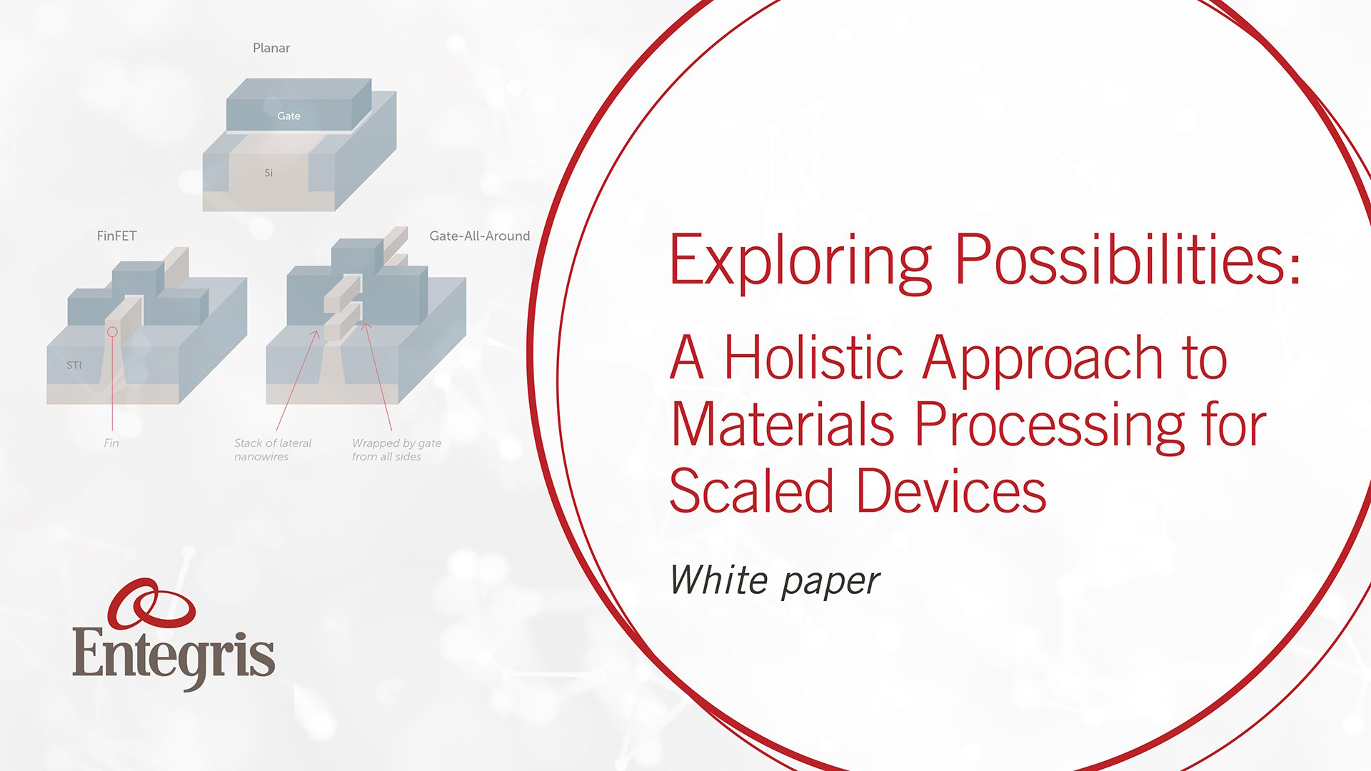
This paper focuses on the issues of scaling logic devices as the industry progresses beyond the 7 nm process node, and the need for changes in device architecture, feature dimensions, process materials, and fabrication equipment to achieve production goals.
INTRODUCTION
The desire for ever more computing power in a smaller footprint requires transistors that perform faster while consuming less power. However, new materials and architectures developed with these goals in mind are not easy to transfer from research and development (R&D) to full-scale, high-volume production.
Manufacturing advanced semiconductor node devices with complex geometric structures is fraught with challenges due to their 3D structures, high-aspect ratios, and nanoscale dimensions. Ultimately, success will be defined by how fast device manufacturers can innovate to simultaneously achieve high performance, high yield, and low cost. But this cannot be accomplished in a silo and requires strong partnerships across the entire supply chain and semiconductor ecosystem.
As the industry progresses beyond the 7 nm process node, changes in device architecture, feature dimensions, process materials, and fabrication equipment are required to achieve production goals. Changes to materials and processes to solve challenges in one part of the fabrication sequence, however, can require corresponding downstream process step changes.
Semiconductor device manufacturers must therefore partner closely with suppliers of everything from metals to etchants to fully understand all the implications of migrating to demanding materials and architectures with challenging geometric constraints.
The issues of device miniaturization apply to both memory and logic devices. This white paper will focus on scaling of logic devices. To read more on the implications for 3D NAND structures click here.1,2.
Learn more about our Holistic Approach to Material Processing for Scaled Devices.


