
This paper highlights some of the new stacking related challenges and proposes solutions to allow designers to increase the number of layers in 3D NAND structures to 96 and beyond.
Introduction
We have reached an era in which a wide variety of computing applications are demanding a doubling of digital storage capacity every 1.5 years. Social media, video and photograph storage, memory sticks, storage centers, and data analytics are putting pressure on chip manufacturers to increase memory density. Demand fuels innovation, and the shift from 2D to 3D NAND storage is a clear example.
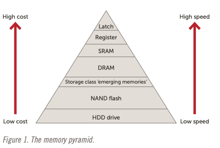
Multiple types of memory are available to satisfy various market demands. The memory pyramid (below) illustrates this well. At the top of the pyramid, the applications require fast embedded devices, while at the bottom the requirements demand less speed but require low cost. NAND memory resides in the middle below DRAM. In terms of requirements, NAND stands alone —it needs to be quite fast, but also low cost. The NAND architecture, which is read in strings of cells rather than individual cells, is most useful when storing large amounts of data such as video, photographs, and documents.
In the same way that population density is greater in high-rise buildings than in single story houses, the pressure to increase the number of bits stored in a given area resulted in a shift from 2D to 3D NAND storage during the past decade. From a device fabrication point of view, this replaced the challenges of shrinking device dimensions with stacking challenges (Table 1). The transition to 3D NAND also allowed an important added benefit, which is the Gate All Around (GAA) geometry. This helps with the fundamental issue of shrinking gate size—running out of material to store sufficient charge.


