Considerations for Improving 3D NAND Performance, Reliability, and Yield
White Paper
NAND flash technology has provided the world with nonvolatile memory capability for many years. Its uses have grown from flash drives to applications in laptops, smartphones, tablets, and solid-state devices now used in cloud storage operations. Over time, its structures have changed to meet growing needs for storage capacity, scale, and reliability demands, but the technology has proven its worth by delivering increased performance and lower power consumption with the promise of a lower cost per bit than previous solid-state memory technologies.
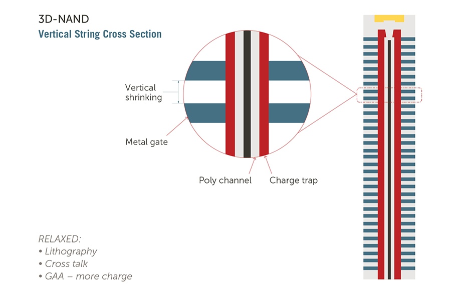
Initially, increased memory density and the corresponding cost reduction resulted from NAND flash memory manufacturers use of multiple patterning techniques to achieve progressively smaller dimensions. Unfortunately, 2D/planar NAND flash memory reached its scaling limit at the 15 nm node. This forced manufacturers to adopt a revolutionary approach of stacking gate-all-around NAND cell layers to achieve new performance targets. This was the dawn of today’s 3D NAND structures, which represent a fundamental shift in the approach to scaling. Instead of scaling horizontally on a two-dimensional plane, this technology introduced vertical scaling, or growth in a third dimension. The promise of 3D NAND is higher density and a lower cost per bit.
With all its promising advantages, however, the process complexity and capital intensity of 3D NAND manufacturing add to the challenges fabs are facing in terms of process control, yield, and economics. With heavy investments, manufacturing processes for 24-layer, 32-layer, and 48-layer 3D NAND were developed in the hope of realizing competitive cost- per-bit. By many accounts, 64-layer and higher 3D NAND structures appear to be where the highest potential for cost savings occurs.


