
DRAM Device Fabrication:
material challenges
DRAM architecture has remained virtually unchanged for the past decade, with the dimensions shrinking proportionally with each successive device node. This linear path, however, is reaching its limits for nodes below 20 nanometers (nm) including 1x, 1y, 1z, 1a, and 1b. A major change will be needed soon if DRAM is to keep up with advances in logic.
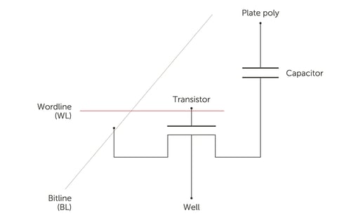
Basic DRAM structure
DRAM fabrication will need to evolve to meet the demands of high-performance devices over the next few years. Next-generation DRAM cells will need new materials and architectures to address the challenges that device shrinking poses. In this paper you will learn about potential solutions:
- capacitor scaling,
- structure and materials changes (dielectric and electrode),
- replacing the wordline metal,
- changing to 3D transistor,
- and replacing DRAM for an emerging nonvolatile memory cell.
Making significant changes will require chipmakers to carefully consider tradeoffs between,
- speed,
- cost,
- and endurance.
Add into the mix the evolving architecture of more memory-centric computing, and this complex system makes it difficult to make any precise predictions.


