
Developing Advanced
Deposition Materials:
a recipe for success
We live in an increasingly connected world that has developed an almost unquenchable thirst for data. To process this raw data into something that is actionable requires the most advanced artificial intelligence (AI) chips for a multitude of applications, from machine learning and autonomous vehicles, to smart cities and efficient energy sources. The quest to develop these devices is driving integrated device manufacturers (IDMs) to push semiconductor manufacturing technology to its very limits.
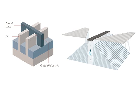
Scaling to smaller device nodes and creating vertical structures are driving completely new paradigms in materials deposition for both logic and memory device manufacturing. In this paper, we will investigate:
- how requirements for deposited film conformality are driving changes in process technology from chemical vapor deposition (CVD) towards pulsed CVD and atomic layer deposition (ALD)
- methods for developing and qualifying customized deposition materials that meet the needs of IDMs and OEMs
- the steps required for ramping to high-volume manufacturing (HVM)
Meeting the challenges of future device nodes and complex structures require innovation, creativity, and inter-company collaboration. A holistic and iterative approach toward new product development is the preferred way to manage the development of precursors for next-generation ALD and CVD processes. This means working collaboratively with both IDMs and OEMS in a very fast-paced and competitive environment. New materials development, as well as packaging, transport, and delivery system optimization must all be considered.


